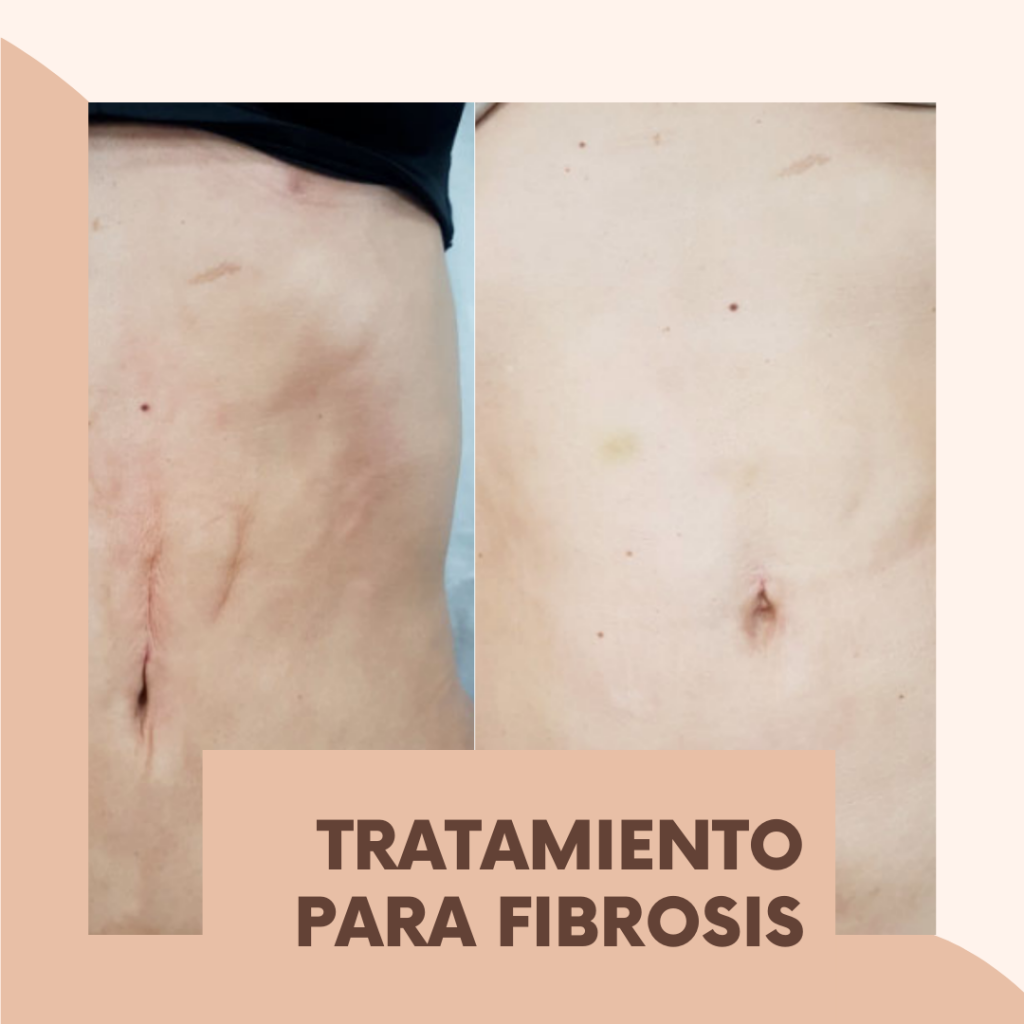
Home

approfondir Pathologique Accusation laser wafer méditation Pâtes Égoïsme

Multilayer stack materials on silicon-based wafer dicing processes using  ultraviolet laser direct dicing and milling methods - ScienceDirect
Multilayer stack materials on silicon-based wafer dicing processes using ultraviolet laser direct dicing and milling methods - ScienceDirect

3DOF / XY-Theta Stages Support Laser Assisted Wafer Slicing

Micromachines | Free Full-Text | Laser Grinding of Single-Crystal Silicon  Wafer for Surface Finishing and Electrical Properties
Micromachines | Free Full-Text | Laser Grinding of Single-Crystal Silicon Wafer for Surface Finishing and Electrical Properties

Singulation, the Moment When a Wafer is Separated into Multiple  Semiconductor Chips | SK hynix Newsroom
Singulation, the Moment When a Wafer is Separated into Multiple Semiconductor Chips | SK hynix Newsroom

Laser Dicing Technique Cuts Wafers from the Inside Out | Features | Jan  2008 | Photonics Spectra
Laser Dicing Technique Cuts Wafers from the Inside Out | Features | Jan 2008 | Photonics Spectra

High repetition rate laser beam measurement for wafer dicing manufacturers

Micromachines | Free Full-Text | Precision Layered Stealth Dicing of SiC  Wafers by Ultrafast Lasers
Micromachines | Free Full-Text | Precision Layered Stealth Dicing of SiC Wafers by Ultrafast Lasers

Silicon Wafers Laser Micromachining - Silicon Wafer Cutting

Semiconductors & Wafer | Micro-Epsilon

Laser processing of doped silicon wafer by the Stealth Dicing | Semantic  Scholar
Laser processing of doped silicon wafer by the Stealth Dicing | Semantic Scholar

Wafer analysis of laser grooving

Dicing by Laser (Laser Dicing) | DISCO Technology Advancing the Cutting Edge

Conventional laser processing (left) vs. full-wafer processing and... |  Download Scientific Diagram
Conventional laser processing (left) vs. full-wafer processing and... | Download Scientific Diagram

Automated analysis of laser grooves on wafers - Clemex

Laser Heating of a Silicon Wafer

355nm UV Laser Has Little Thermal Effect And Is Used For Cutting Silicon  Wafers
355nm UV Laser Has Little Thermal Effect And Is Used For Cutting Silicon Wafers

Water jet guided Laser MicroJet for semiconductor industry

Silicon wafer laser scribing: laser technology with no substrate chipping -  Toolas
Silicon wafer laser scribing: laser technology with no substrate chipping - Toolas

Micromachining a Silicon Wafer - Laser Impressions Inc.

Plasma Dicing 101: The Basics | Innovation | KLA

Wafer Laser Marking - E&R Engineering corp.

Laser Cutting Silicon Wafers

Semicon wafer laser marker - Hylax Technology Laser Solution Provider

WB-300FGS - E&R Engineering corp.

Semicon wafer laser marker - Hylax Technology Laser Solution Provider